Table of Contents
Toggle- The 8051 has two types of memory and these are Program Memory and Data Memory.
- Program Memory (ROM) is used to permanently save the program being executed, while Data Memory (RAM) is used for temporarily storing data and intermediate results created and used during the operation of the microcontroller.
- Let’s have a brief detail of memory organization of 8051 microcontroller.
- Depending on the model in use 8051 microcontroller family in general have at most a few KB of ROM and 128 or 256 bytes of RAM is used.
- All 8051 microcontrollers have a 16-bit addressing bus and are capable of addressing 64 kB memory.

Program Memory Organization of 8051
- The first models of the 8051 microcontroller family did not have internal program memory. It was added as an external separate chip.
- Even though such an amount of memory is sufficient for writing most of the programs, there are situations when it is necessary to use additional memory as well. A typical example is so called lookup tables.
- They are used in cases when equations describing some processes are too complicated or when there is no time for solving them. In such cases all necessary estimates and approximates are executed in advance and the final results are put in the tables (similar to logarithmic tables).

EA=0 In this case, the microcontroller completely ignores internal program memory and executes only the program stored in external memory.
EA=1 In this case, the microcontroller executes first the program from built-in ROM, then the program stored in external memory.
- In both cases, P0 and P2 are not available for use since being used for data and address transmission. Besides, the ALE and PSEN pins are also used.
Data Memory Organization of 8051
As already mentioned, Data Memory is used for temporarily storing data and intermediate results created and used during the operation of the microcontroller. Besides, RAM memory built in the 8051 family includes many registers such as hardware counters and timers, input/output ports, serial data buffers etc.
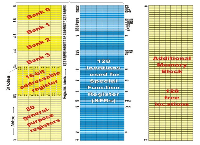
The previous models had 256 RAM locations, while for the later models this number was incremented by additional 128 registers. However, the first 256 memory locations (addresses 00-FFH) are the heart of memory common to all the models belonging to the 8051 family.
Locations available to the user occupy memory space with addresses 00-7Fh, i.e. first 128 registers. This part of RAM is divided in several blocks.
The first block consists of 4 banks each including 8 registers denoted by R0-R7. The PSW has two bits for identifying the register bank, i.e., 00 represents bank 0, 01 represents bank 1, 10 represents bank 2, and 11 represents bank 3.
Prior to accessing any of these registers, it is necessary to select the bank containing it.

The next memory block (address 20H-2FH) is bit- addressable, which means that each bit has its own address (0-7FH). The bit-addressable memory is both bit-addressable (from 00H to 7FH) and byte-addressable (from 20H to 2FH). Bit operations are helpful in many control algorithms.
The third group of registers occupies addresses 2FH-7FH, i.e. 80 locations, and does not have any special functions or features.
Special Function Registers (SFRs)
- SFR, which occupies upper 128 bytes of internal memory are the registers, that control the entire processor
- They can be accessed by DIRECT addressing.
The registers available in the 8051 are as follows:
- Accumulators – A and B
- Process Status Word – PSW
- I/O port registers – P0, P1, P2, P3
- Data pointers – DPH and DPL
- Serial data buffer register – SBUF
- Stack pointer – SP
- Timer registers – TH0, TH1 and TL0, TL1
- Timer Control Registers – TCON, TMOD
- Power and Port control – PCON, SCON
- Interrupt Control Registers – IP, IE.
- Programmers should not use the addresses in the range 80H to FFH (other than SFR) as it is used by INTEL CORPORATION for expansion functions of 8051.
Additional RAM
- An additional memory block of 128 locations is added into the latest versions of the 8051 microcontrollers. The problem is that electronics performing addressing has 1 byte (8 bits) on disposal and is capable of reaching only the first 256 locations, therefore.
- In order to keep already existing 8-bit architecture and compatibility with other existing models a small trick was done. It means that additional memory block shares the same addresses with locations intended for the SFRs (80H- FFH).
- In order to differentiate between these two physically separated memory spaces, different ways of addressing are used. The SFRs memory locations are accessed by direct addressing, while additional RAM memory locations are accessed by indirect addressing.


each time i used to read smaller articles or reviews which as well clear their motive, and that is also happening with this post which I am reading at this time.